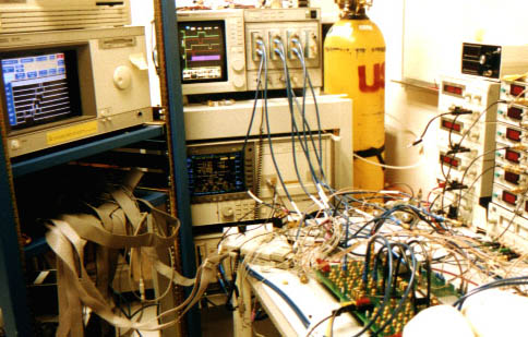
The multi-processor system is composed of 16 nodes, each having four 4x64 multiplexed backplane switches. Each switch supports four Electrical I/O Ports and 64 optoelectronic input and output paths, and each port/path consists of 12 bits signalling at 1.0 Gb/s. The network is locally controlled by means of a busy-bit monitoring scheme. USC's Advanced Interconnect and Network Technology Laboratory is responsible for the development, test and evaluation of test circuits which will be used in the switched backplane IC.
 |
 |
|
|
|
Reports and publications
TE01: (1.25 Gb/s, 0.5 mm) Receiver / Transmitter test
Evaluation of a low-power, 1.25 Gb/s, LVDS sense-amp receiver (demuxed) design to operate at 30% conventional receiver power consumption.TE02: (2.0 Gb/s, 0.35 mm) 32 Gb/s 4-port Switch IC
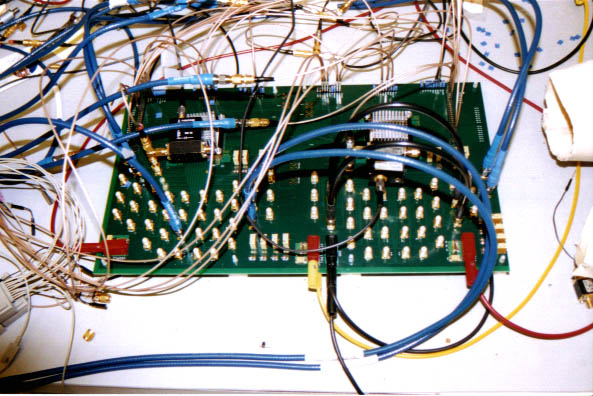
The TE02 Switch IC is implemented in 0.35 mm HP CMOS process and operates at 2.0 Gb/s to fully connect 4 processors with a peakthroughput of 32 Gb/s. The TE02 IC contains two LVDS 4-b electrical I/O interface ports representing the electrical I/O interface of a scaled-up Switch IC. It also contains two separate LVDS 4-bit electrical input and output paths representing the optoelectronic interface of such a scaled-up IC. TE02 also includes BUSY BIT monitoring circuitry to monitor the processor status.TE03_35: (2.25 Gb/s, 0.35 mm) 36 Gb/s 4-port Switch ICThe Rx portion of the IC contains a higher speed, more robust version of the sense-amp circuitry used in TE01. The IC operation includes physical loop back as well as a 4-b wide, 2-path all-electrical interconnection network
The TE03_35 is a revised version of the original TE02 switch IC implemented in 0.35 mm CMOS process and operates at 2.25 Gb/s to fully connect 4 processors with a peakthroughput of 36 Gb/s. The TE03_35 IC contains two LVDS 4-b electrical I/O interface ports representing the electrical I/O interface of a scaled-up Switch IC. It also contains two separate LVDS 4-b electrical input and output paths representing the optoelectronic interface of such a scaled-up IC. TE03_35 also includes BUSY BIT monitoring circuitry to monitor the processor status.TE03_25:(3.0 Gb/s, 0.25 mm) 48 Gb/s 4-port Switch ICThis design was used in the FRPA-Network demonstration.
The TE03_25 is a revised version of the original TE02 switch IC implemented in 0.25 mm CMOS process and operates at 3.0 Gb/s to fully connect 4 processors with a peakthroughput of 48 Gb/s. The TE03_25 IC contains two LVDS 4-b electrical I/O interface ports representing the electrical I/O interface of a scaled-up Switch IC. It also contains two separate LVDS 4-b electrical input and output paths representing the optoelectronic interface of such a scaled-up IC. TE03_25 also includes BUSY BIT monitoring circuitry to monitor the processor status.BUSY BIT #1: (3.0 Gb/s, 0.25 mm) Quarter micron isolated BUSY BIT test IC.
The BUSY BIT IC #1 is implemented in 0.25 mm CMOS technology. This is a direct scale (with slight modifications to the grab RS output latches for process changes from 0.35 mm to 0.25 mm) of the BUSY BIT circuits that were included in the TE02 IC. The purpose of the IC is to test the scaling of the circuitry and the BUSY BIT logic to smaller feature sizes.TIA: (2.5 Gb/s , 0.35 mm) Single analog TIA
The TIA designed in 0.35 mm technology has
a BER < 10-13 (231-1 NRZ PRBS, 22 mA
input current) and a phase margin of 50% (30 mA
input current) for a signal data rate of 2.5 Gb/s. The TIA, amplifiers
and drivers consumes 160 mW.
![]()